|
|
|
|
OTHER ELECTRONICS
UPDATE
February 2007
McIlvaine Company
New Semiconductor Test Methods
Livermore-based FormFactor Inc. manufactures a semiconductor test method that has so influenced the way semiconductors are produced that chip makers around the world are buying up its product. That has given FormFactor a 55 percent yearly revenue growth rate for the past three years and a name in the Smithsonian, where the company's product is displayed among a collection of technologies that have made big differences in our time. And, it has won FormFactor a big following on Wall Street. Pundit The Motley Fool has called it the "Best Small Cap for 2007" and investors have tripled the price of the stock since FormFactor went public in 2003. Last week, it traded at $42.85.
FormFactor invented a MEMS-based wafer probe card, which is used by semiconductor chip makers to test silicon wafers for their electrical circuitry performance.
While the name conjures up images of cookies and cardboard, wafer probe cards are actually highly designed, electronics-driven and silicon-based products that allow delicate testing or "probes" of silicon wafers, the wafers of circuitry-etched silicon that eventually become chips. Wafer testing is a critical and often repeated step along the many highly sensitive processes that go into making semiconductor chips.
In a sprawling manufacturing "fab" in Livermore, close to 1,000 technicians, cleanroom operators, engineers and others manufacture the wafer probe cards in a 125,000-square-foot factory that FormFactor built for $750 million over the past three years.
Khandros' technology is based on MEMS, or micro-electrical mechanical systems, extremely small electrical mechanical devices that can move equipment by distances so small that the human eye cannot see the movement. MEMS is the next best thing after nanotechnology in sciences for which small is better.
For chip makers, small is the holy grail. Reducing the size of a chip while maintaining or increasing the computations it can perform by adding more circuitry has been an ongoing pursuit of the industry. Chip makers such as Intel Corp. and Samsung Corp., two of FormFactor's major customers, bet their existence on making small but high performance chips. With such chips they can put computers into such devices as digital cameras, mobile phones, BlackBerries and portable MP3 players that also play video. Processing video and sound are among the most computationally heavy demands a chip is asked to make. Chip makers can shrink powerful chips that handle video and audio because of technologies like FormFactor's, analysts said.
Semiconductor equipment makers, whose production facilities are smaller than semiconductor makers, have been trying to hold on to manufacturing in California, but very few do all of their manufacturing here. The headquarters, product design and engineering as well as the research and development operations of major equipment makers such as Applied Materials Inc., Lam Research Corp. and Novellus Systems Inc. still reside in the Silicon Valley cities of Santa Clara, Fremont and San Jose, respectively. Many other equipment makers are based in Fremont. But industrywide, companies do the bulk of their manufacturing elsewhere, bringing parts together for final assembly here, analysts and industry participants say.
"We probably built the last semiconductor fab (manufacturing plant) in California," Khandros said. But he added it is also the last FormFactor will build in California because it faces the same competitive pressures as others in the semiconductor equipment industry. Construction on the $750 million plant started in 2003 and was completed last year.
Since most semiconductor manufacturing is now done in Asia, FormFactor is a net exporter of its products, with 70 percent of its sales in Asia.
The Semiconductor Equipment Association of Japan reported that worldwide sales for all semiconductor equipment and test manufacturers rose 23 percent in 2006 to $40.5 billion — its highest level since the technology boom of the late 1990s and year 2000. Demand was driven by consumers wanting mobile phones, portable digital music players and by the computer manufacturers making new designs ahead of the release of Microsoft Corp.'s Vista operating system.
Semiconductor equipment makers are the first part of the electronics food chain. They feed semiconductor makers, which in turn feed computer makers and mobile phone and electronic device makers.
FormFactor's highly patented MicroSpring interconnect technology lets chip makers test a wafer's viability and performance for different jobs, such as that of DRAM or microprocessing. Because FormFactor's technology does this testing or probing when the chips are still in wafer stage and not yet separated and packaged into individual chips, it has driven down the cost of making chips and driven up the yield of good chips that come out of a wafer supply. It also allows many more chips to be tested at once — 250 to 300 chips at once compared with about 50 chips under old technologies.
But FormFactor does have risks and shadows in its closet. One is that other test equipment makers have started to mimic its invention and may eventually dent its 70 percent market dominance in wafer testing.
Sungkyunkwan University's Seoul Campus
This medical department has escalated to be in the top class nationally with its spacious facilities and good scholarship programs. The university's medical department now has a 90,000-pyeong (297,000-square-meter) building in Suwon with 395 full-time faculty members and 539 undergraduate and graduate students. Before the college was established, the Samsung Medical Center, which sits on about 60,000 pyeong of land, was constructed in Ilwon-dong, southern Seoul, in November 1994.
The Suwon campus, for natural science majors, was built in 1981.
With Samsung's support, the university was able to complete a school with upscale facilities and introduce pioneering new programs, such as semiconductor engineering and cellular phone studies majors.
One hundred students are accepted every year on the Samsung-sponsored program and freshmen receive basic grounding in areas including physics, chemistry and calculus. Practical training begins the following year and numerous leadership courses, including global marketing, are offered. More than 50 percent of the classes are held in English.
Gigaphoton Opens Facility at Headquarters Campus in Japan
Gigaphoton Inc of Japan has completed construction of a new building at its headquarters campus. Slated to open February 1, this new facility will house a Class-1,000 cleanroom that features expanded research and development capabilities and laser light source maintenance training for field service engineers.
With training and R&D transitioned to the new facility, the existing building will now be fully dedicated to production of the company's advanced laser systems. This will enable the company to nearly double its manufacturing capability as early as April.
In addition to the expanded cleanroom area for research and development activities, the training facilities have increased significantly. This expansion investment will allow the company to further augment its customer support capabilities to address its growing installed base. The new facility will also house the company's customer support administrative functions, as well as a spare parts warehouse.
Nextest to Expand Headquarters at New Facility in San Jose, CA
Nextest Systems Corporation, a leading manufacturer of automatic test equipment (ATE) for cost-sensitive semiconductors, announced that it will establish its new corporate headquarters at 5345 Hellyer Avenue in San Jose, CA. The new 128,000 square foot facility, located in the city's Edenvale district, offers more than twice the capacity of the
current facility. Plans for the new building include a state-of-the-art manufacturing floor, increased facilities for research and development, as well as expanded training and customer conference rooms to facilitate meetings with customers and business partners. The new facility is currently targeted to be ready for occupation in September 2007.
ESI’s Newest Cleanroom Paves the Way for Future Growth Opportunities
Electro Scientific Industries, a leading provider of world-class production laser systems for microengineering applications, announced the completion of its newest cleanroom located at the company’s corporate headquarters in Portland, Ore. The new cleanroom encompasses both a Class-1000 as well as a Class-100 cleanroom, and adheres to both the federal 209E and the ISO 14644-4 standard. ESI believes the new facility’s state-of-the-art manufacturing capabilities enable ESI to develop solutions with compelling yield advantages for its customers, while addressing their evolving requirements for leading-edge solutions.
Following the Class-1000 R&D cleanroom, built in 2004, this new facility, dedicated primarily to production, was developed to accommodate the industry’s move to revolutionary applications. Construction of the new cleanroom began in January of 2006, and became fully operational by the end of the year. The addition of the new ISO 14644-4 cleanroom furthers ESI's ability to respond to its customers’ demand for innovative solutions that enable significant yield improvement.
ESI is a pioneer and leading supplier of world-class production laser systems that help its microelectronics customers achieve compelling yield and productivity gains. The company's industry-leading, application-specific products enhance electronic-device performance in three key sectors — semiconductors, components and electronic interconnect — by enabling precision fine-tuning of device microfeatures in high-volume manufacturing environments. Founded in 1944, ESI is headquartered in Portland, OR.
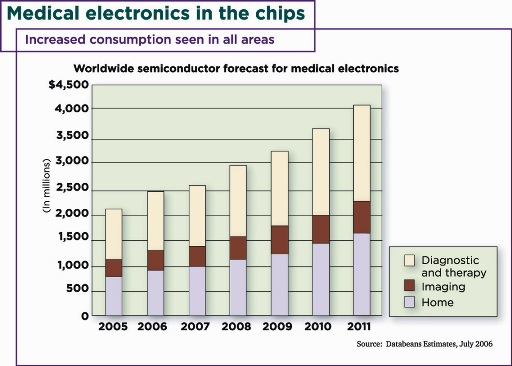
Electronics Gears for Health Care Innovation
Biomedical research is making huge strides in unlocking the secrets of human physiology and identifying potential new therapeutic and diagnostic instruments. At the same time, advances in electronics are enabling those new devices to be realized. As a result, medical applications make up one of the fastest-growing segments for ICs. The growing convergence of electronics and medicine can also be seen in trends that are common to both disciplines. While it may seem that the two fields have little in common, they actually share several technological frontiers: Both are driven by the need for small physical size, low power and advanced connectivity.
Some medical devices require the maximum possible processing power. Radiological and magnetic imaging systems consume all the gigaflops they can get, and size is not the main concern. In other applications, however, computing requirements are more modest, and there's no room for large components. The enabling factor in these devices is getting enough processing power into a given space.
Size matters
The space allowed for a medical device can be subject to some interesting constraints. Diabetics use glucose meters to monitor their blood sugar. Typically, these portable electronic medical devices are about the size and shape of a PDA, where the user inserts a test strip with a drop of blood. Using an electrochemical or optical sensor, these meters determine the concentration of glucose in the blood. One company has created a meter small enough to be integrated into the cap of the pill bottle-size canister that holds the test strips. The sensor, MCU, LCD and battery all fit into a finished product roughly the size of a ladies' wristwatch. Small size has also yielded low cost, as the meter is disposable — after the 50 strips are used, the container is thrown away, meter and all.
In the case of implanted devices, size is also important in determining where they can be placed. Consider an aortic aneurysm, which occurs when the heart's main artery, the aorta, develops a weak spot and bulges from blood pressure. A common surgical treatment is to run an artificial liner, called a stent graft, through the weakened aorta. It's now possible to place a tiny pressure sensor inside the aorta at the same time. The sensor uses a MEMS pressure element to monitor the long-term success of the surgery.
The MEMS sensor is made using the same processing technologies as ICs. To read the pressure in the aorta, the surgeon uses a radio-controlled interrogator to activate the device, which transmits via RF. If the stent graft fails, a follow-up exam will show increased pressure, indicating the need for further intervention. Some other implanted devices that benefit from smaller size are cardiac pacemakers, neurostimulators for treating central nervous system disorders, and hearing aids, including cochlear implants.
One of the most fascinating applications to exploit the mutual shrinking of medical devices and electronics is the sensor that's designed to be swallowed like a pill. Using RF, these minute instruments travel the full length of the digestive system during their operating lifetimes. The first such sensor transmitted body temperature, and has been used by astronauts and athletes. Newer versions can report pH levels in the esophagus to diagnose acid reflux disease and other conditions.
With innovation in electronics and medicine aligning around miniaturization, low power and connectivity, the development of new electronic medical devices is expected to accelerate. The very latest devices transmit still images, which can be assembled into video, allowing a doctor to examine the small intestine. The "camera pills" use a minute CMOS imager coupled to an ASIC transmitter. White LEDs surrounding the lens provide illumination. Early work is being done on next-generation ingestible devices, incorporating navigation control and self-propulsion to allow more detailed imaging of a particular site.
Portability, power
Along with miniaturization is the trend toward lower power. In an implanted device, the benefit of minimal current consumption and the resulting impact on battery life are obvious. While some implants can be recharged through the skin with inductive coupling, less battery drain is always a desirable objective.
External devices are also sensitive to power consumption. As electronic components get smaller, medical devices that were once stationary are becoming portable. Defibrillators were once used only in hospitals by trained professionals. Automatic external defibrillators are now commonplace in airports, shopping malls, schools and even on airliners. Portable oxygen concentrators extract oxygen from the air for patients on oxygen therapy and can be carried over the shoulder like a handbag. All of these devices are enabled by low power, in addition to small size. Their tight power budgets are met by various means.
Ironically, reducing the size of electronic components can actually work against power reduction. As transistors get smaller to allow greater density, effective channel lengths get shorter and leakage current increases. Other mechanisms such as gate tunneling have a similar adverse impact on power as geometries shrink. With each geometric reduction, chipmakers have countered these negative effects by optimizing silicon-processing parameters. In addition, the designers of both digital and analog chips spend time minimizing the power consumption of their circuits. Reducing supply voltage, managing capacitance, clock gating and other techniques are used to eliminate unnecessary current.
Chip designers also incorporate features into their parts to allow medical device designers control over power consumption. For example, the dsPIC33F family from Microchip Technology has idle, sleep and doze modes, each with multiple options, giving designers the flexibility to scale power consumption. In many medical devices, an MCU spends most of its time doing nothing.
The inputs to vital sign monitors, infusion pumps, data recorders and many diagnostic instruments are fairly slow-moving temperatures, pressures and bioelectrical signals. Processors in such devices can remain in a low-power state most of the time, waking up every few milliseconds to execute instructions. In this way, the total average current is a fraction of the processor's normal run current.
Further progress in the area of power conservation will enable the development of new classes of devices. Piezoelectric or thermoelectric power sources may someday replace batteries in some implants. Already, a microsensor has been built into a hip implant to monitor the integration of the implant into the healing bone tissue. The device is kinetically powered, using the patient's movement as its energy source.
Connectivity trend
The third trend shared by electronics and medical devices is connectivity. In both fields, wireless is the leading technology. In 1999, the FCC allotted a bandwidth of 402-405MHz to the Medical Implant Communication Service. This band is used to communicate with implanted devices such as a pacemaker.
Other external devices use Bluetooth, IR, the Zigbee protocol, Wi-Fi or proprietary protocols to communicate. Home health-care networks connect weight scales, blood pressure cuffs, thermometers, spirometers and other diagnostic instruments to telemedicine terminals. These networks allow effective disease-management care without frequent trips to a doctor's office.
Of course, not all medical networks are wireless. Some devices are complex enough to make use of their own internal networks. For example, a dialysis machine may contain a dozen or more MCUs. Wired and wireless LANs are getting busier in hospitals as well. Electronic patient records, prescription ordering and delivery, and imaging data can all be made available online or at the patient's bedside.
With innovation in electronics and medicine aligning around miniaturization, low power and connectivity, the development of new electronic medical devices is expected to accelerate. At the same time, it's appropriate to be mindful of the challenges presented by differences between the two fields. The rate of change in ICs is far more rapid than in medical devices. Component suppliers naturally prefer to offer their newest products, built on their newest processes. On the other hand, the designer of a medical device typically prefers to design in a component after it has been on the market for a while and established a track record. Similarly, by the time a medical device has passed the review and been released to production, the manufacturer is generally reluctant to accept changes to components.
In the end, an ongoing convergence of medical and electronics technology is inevitable. Biomedical research is continuing to identify new treatments for disease. Electronics research is likely to continue to enable the development of devices to apply those treatments. Greater cooperation between engineers in the two fields will advance health care in ways barely imaginable today. Steve Kennelly
|
|
|
|
Magma Expands in India
EDA provider Magma Design Automation Inc. has moved to new facilities in India and the U.S. in anticipation of expanding staff and operations in both regions.
The company's Bangalore, India operation is moving to a new 40,000 square foot facility. It's one of three facilities that Magma currently has in India, including Noida and Mumbai (Bombay), which was added with the November 2006 acquisition of Knights Technology. Magma has over 200 employees in India and expects to expand in this region. Meanwhile, in the United States, Magma is relocating its corporate headquarters from Santa Clara, CA. to new offices in San Jose, CA.
Legend Silicon Open Shanghai Design Lab
Analog Devices Inc. (ADI) and Legend Silicon Corp. announced the opening of a joint design laboratory to develop reference designs for China's emerging mobile TV market.
The design lab located in Shanghai, will provide complete front-end solutions, from the antenna through the tuner to the demodulator to the MPEG2 TS interface, to allow OEMs and ODMs to quickly equip their mobile terminal product — including portable media players, PDAs, laptop PCs, automotive displays and smart phones — to receive terrestrial digital TV broadcasts.
McIlvaine Company,
Northfield, IL 60093-2743
Tel: 847-784-0012; Fax: 847-784-0061;
E-mail: editor@mcilvainecompany.com;
Web site: www.mcilvainecompany.com